PCB Transport Blister Tray for Circuit Board Handling and Packaging
A PCB transport blister tray provides designated positions for circuit boards during handling, storage, and transport. Custom cavities can be developed around board dimensions, approved support areas, and component clearance requirements.
WELL CHSIEN PLASTIC CO., LTD. manufactures custom vacuum-formed trays in Taiwan, including electronic work trays, antistatic trays, and conductive trays. Our services include drawing and sample evaluation, material selection, mold development, sampling, and production.
For PCB and PCBA packaging, a suitable tray must address both mechanical fit and the intended handling environment. The design should support the board without placing unwanted pressure on components, solder joints, connectors, or other sensitive features.
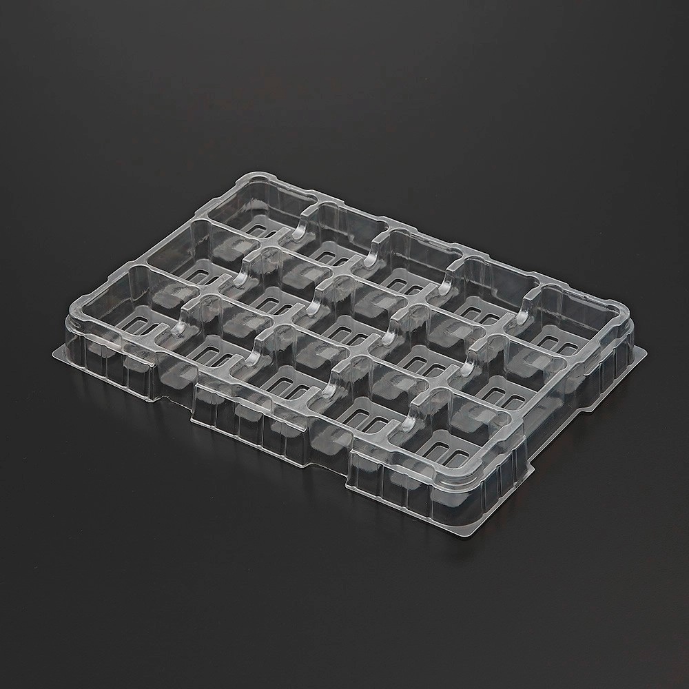 Clear PCB transport blister tray with deep rectangular compartments, raised dividers, and rounded access recesses
This PCB transport blister tray features deep individual compartments and rounded access recesses for organized placement and manual handling. Custom development can address approved board support areas, underside component clearance, and cavity spacing. WELL CHSIEN evaluates drawings and samples to match the tray geometry to the actual PCB or PCBA configuration.
What Is a PCB Transport Blister Tray?
A PCB transport blister tray is a thermoformed plastic tray with one or more cavities designed to accommodate printed circuit boards. In this application, “blister tray” describes the formed packaging structure; it does not necessarily indicate a sealed retail package.
The requirements differ between a bare PCB and a populated printed circuit board assembly, or PCBA.
A bare board may require separation and protection of its surfaces and edges. A populated assembly also needs clearance around mounted components, projecting terminals, and features on the underside.
Providing the complete board geometry helps establish a practical design from the beginning.
| Packaging item | Main design considerations |
|---|---|
| Bare PCB | Board outline, surface contact restrictions, and separation |
| Single-sided PCBA | Component height, underside features, and support locations |
| Double-sided PCBA | Clearance and approved contact areas on both sides |
| Board with projecting connectors | Additional space around connector bodies and terminals |
| Board with a battery | Electrical contact restrictions and applicable transport requirements |
Explore our electronic work trays for related circuit board handling applications.
Board Support and Component Clearance
The board outline is only part of the information needed to design a tray.
Support locations should be approved by the customer’s engineering team. Depending on the assembly, suitable areas may include designated board edges or other defined contact zones. Components and solder joints should not become unintended load-bearing points.
For example, a double-sided assembly may need raised supports beneath approved areas, with recessed spaces around underside components. A projecting connector may require an extended cavity rather than a close-fitting rectangular pocket.
Important dimensions include:
-
Board length, width, thickness, and tolerances.
-
Maximum component height above and below the board.
-
Connector and terminal projections.
-
Approved support locations.
-
Areas where tray contact is prohibited.
-
Clearance needed for loading and removal.
A sample should be checked with the actual board assembly, including its tallest components and relevant dimensional variations.
Cavity Layout for Loading and Inspection
The cavity layout should balance packing density with practical handling.
Placing more boards in a tray can reduce the number of trays required, but adequate spacing is still needed for component clearance and operator access. Finger recesses can help operators reach approved board edges without pulling on connectors or mounted components.
Orientation features can also help establish a consistent loading direction. If different board versions share a tray, each version should be evaluated rather than assuming that a similar outline guarantees compatibility.
| Tray feature | Purpose | What to verify |
|---|---|---|
| Individual cavities | Separate neighboring boards | Clearance between assemblies |
| Support platforms | Hold boards at approved locations | Contact position and loaded stability |
| Finger recesses | Assist manual removal | Access without contacting sensitive parts |
| Connector recesses | Accommodate projecting features | Clearance across product tolerances |
| Orientation features | Indicate loading direction | Compatibility with the board outline |
| Position markings | Identify cavity locations | Readability during actual use |
For automated loading, provide equipment interface drawings, positioning references, gripping areas, and tray separation requirements.
Selecting ESD Materials for PCB Transport
A PCB transport blister tray may require antistatic, dissipative, or conductive material properties, depending on the board’s sensitivity and the handling environment.
These properties describe different functions. Antistatic generally concerns reduced charge generation. Dissipative and conductive properties concern electrical resistance and charge movement. Discharge shielding is a separate packaging function.
The EOS/ESD Association’s principles of ESD control ↗ explain why packaging selection should form part of a wider ESD control program.
An open antistatic or conductive tray should not automatically be assumed to provide adequate discharge shielding. When sensitive assemblies leave an ESD protected area, evaluate whether the complete package needs a suitable shielding enclosure.
| Requirement | Purchasing information to provide |
|---|---|
| Low charging behavior | Intended contact materials and handling process |
| Dissipative or conductive properties | Required electrical limits and measurement method |
| Discharge shielding | Requirements for the complete packaging system |
| Verification | Test conditions, sampling, and required records |
| Service conditions | Storage environment, cleaning, and expected reuse |
Compare our antistatic working trays and conductive working trays when discussing material requirements.
Loaded Stacking and Cover Design
A stack of loaded trays must support its own weight without transferring unintended pressure to the boards.
Stacking features should maintain clearance above the tallest component. Tray deflection, dimensional variation, and the expected stack load should be considered during evaluation.
A cover can help retain the contents, but its design must also avoid component contact. A standard plastic cover does not by itself establish ESD shielding, moisture protection, or a sealed barrier.
| Stacking consideration | Review question |
|---|---|
| Load path | Is the upper layer supported by the tray structure? |
| Component clearance | Is there sufficient space above every assembly? |
| Tray deflection | Does the loaded tray maintain the required clearance? |
| Lateral movement | Can stacked layers shift during handling? |
| Cover fit | Can the cover contact or displace a board? |
| Outer packaging | Does the stack fit the agreed carton and cushioning? |
Evaluate stacking with the intended number of loaded layers, rather than checking empty trays alone.
Material and Thickness Selection
WELL CHSIEN works with vacuum forming materials including PET, PVC, PS, and PP. A suitable grade should be confirmed for the electrical, mechanical, and environmental requirements of each project.
Starting sheet thickness alone does not describe the strength of the finished tray. Cavity depth, formed geometry, material distribution, board weight, and support structure also influence performance.
A transport tray should not automatically be used for baking, reflow, washing, or other processing operations. Those uses require separate confirmation of temperature capability and chemical compatibility.
If moisture protection is required, define the barrier packaging requirements separately. An open thermoformed tray is not a moisture barrier.
Validate the Complete Shipping Package
A tray provides positioning and separation, while shipping performance depends on the complete packaging arrangement.
For external transport, review the loaded tray together with its cover, shielding enclosure where required, cushioning, and outer carton. The evaluation should reflect the actual distribution route and customer requirements.
Sample approval should address fit and handling. Where transport qualification is required, agree on an appropriate test plan and acceptance criteria for the complete package.
Useful checks include:
-
Confirming that boards remain in their intended positions.
-
Checking for contact marks or damage at support points.
-
Inspecting connectors, components, and board edges.
-
Verifying that stacked layers maintain clearance.
-
Confirming the required electrical performance.
-
Reviewing the package after the agreed transport testing.
These checks help identify issues that may not appear during a simple visual inspection of an empty tray.
Custom Development and Quotation Requirements
WELL CHSIEN supports custom tray development from initial evaluation through tooling, sampling, and production.
Provide drawings or samples that represent the actual board configuration. If a board is still under development, identify dimensions that may change before tooling is approved.
| RFQ item | Recommended details |
|---|---|
| Board geometry | Outline, thickness, tolerances, and CAD drawings |
| Assembly profile | Component heights and underside features |
| Contact restrictions | Approved support areas and prohibited contact zones |
| Tray layout | Cavity quantity, orientation, and outer size limits |
| Electrical requirements | Material properties, limits, and test methods |
| Handling | Manual loading, equipment interfaces, and removal method |
| Transport | Internal transfer or external shipping conditions |
| Stacking | Loaded layer count and cover requirements |
| Quantity | Initial order and estimated repeat demand |
| Documentation | Inspection records and material declarations |
Tooling cost, minimum order quantity, sample timing, and production lead time depend on the agreed design and material.
Learn more about our vacuum formed products and industrial tray range.
FAQ: PCB Transport Blister Tray
1. Can one tray hold both bare PCBs and populated assemblies?
Possibly, but each configuration needs evaluation. Mounted components change the required support areas, cavity depth, and clearance. Approval for a bare board does not automatically cover a populated version.
2. How should a PCB be supported inside the tray?
Use engineering-approved contact areas that support the board without loading sensitive components or solder joints. Supply drawings showing permitted and prohibited contact locations.
3. Can a tray accommodate components on both sides of a board?
A custom design can be evaluated with recesses and supports around the assembly profile. Provide component heights on both sides, including terminals and other projections.
4. Should I choose antistatic or conductive material?
Follow the requirements of your ESD control program. The appropriate properties depend on component sensitivity, contact conditions, and the handling environment. Confirm measurable requirements before selecting a material.
5. Does an ESD tray provide complete shipping protection?
The tray is one part of the package. External transport may also require shielding, cushioning, and a suitable outer carton. Evaluate the complete system against the intended conditions.
6. Can loaded trays be stacked?
Stacking can be considered during design. Confirm the number of layers, total load, and required clearance so that the upper trays do not press on the boards below.
7. Can the trays be reused?
Reuse depends on physical condition, cleanliness, and continuing electrical performance. Establish inspection and replacement criteria for the intended returnable packaging process.
8. Can the tray be used for PCB baking or cleaning?
Only after its suitability has been confirmed for the actual process. Transport use does not establish compatibility with elevated temperatures, cleaning chemicals, or repeated processing cycles.
9. What happens if the PCB design changes?
Review the revised board against the approved tray. Changes to connectors, component height, or underside features can affect fit even when the board outline remains unchanged.
10. What is needed to request a quotation?
Send board drawings or samples, assembly height information, tray layout preferences, ESD requirements, order quantity, and delivery expectations. Include stacking and shipping requirements for a more complete review.
Discuss Your PCB Transport Blister Tray Project
WELL CHSIEN provides custom thermoformed packaging development for electronics and industrial applications.
Share your PCB or PCBA drawings to discuss board support, component clearance, material options, and packaging requirements. A clearly defined specification provides the basis for sample approval and repeat production.
Contact WELL CHSIEN to discuss your PCB transport blister tray requirements.
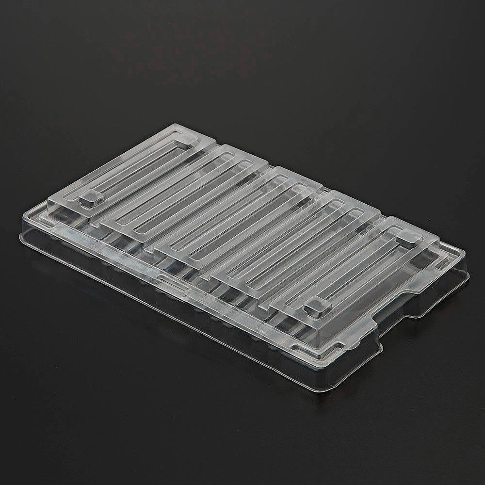 Clear PCB transport blister tray and cover with parallel reinforcing ribs and a raised perimeter
This PCB transport blister tray and cover arrangement features parallel ribs across the top and a formed perimeter. For a custom project, cover clearance and tray support locations should be checked against the loaded assembly. WELL CHSIEN can review board dimensions, component heights, and stacking requirements before sample approval.
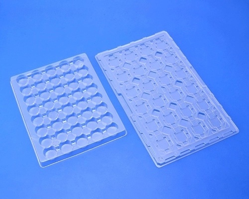 Two clear electronics packaging trays with circular pockets and contoured cavities on a blue background
These thermoformed trays illustrate circular and contoured cavity layouts for organizing electronic parts. Each layout can be evaluated around product shape, separation, and removal access. For a PCB transport blister tray project, cavity geometry should instead follow the board outline, approved contact areas, and clearance around mounted components.